The aim of these pages is to give a clear and simple set of illustrated instructions on how to upgrade your Z88 to the version 4 ROM and to 128/512Kb of internal RAM.
Before You start!
You should collect together all the following components before starting work:
- medium cross-point screw driver.
- A soldering iron and a good quality, large solder sucker.
- A low profile, 32 pin DIL socket (FZ65V)
- The 512Kb pseudo-static RAM chip, (HM658512LP) usually recommended for this upgrade, is now very difficult to obtain. The hardware specification clearly states that Static RAM is not only usable, but better, as it has a much lower current consumption. I started out going for the 128K upgrade, as this works well with the original ROM, so I purchased a KM681000CLP-5L from Radio Spares (RS) on line store. This is a CMOS, low power, 1Mb chip, organised as 128kx8 in a 32 pin DIL. I would recommend the 128K upgrade over the 512 to anyone who is unsure of their soldering skills, as it does not require any modification of the main board, other than the removal of one chip.
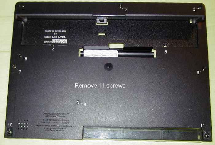
We need to get access to the Z88’s main board, so it must be completely disassembled. This requires the removal of eleven cross point screws in the base of the case. Most are easily visible, but two are beneath the rubber front feet, which must be carefully peeled off, whilst another two are under the pull out support flap. The left one of these is probably hidden under the edge of the serial number label, which can just be bent back enough to release the screw. All of these are highlighted in the following picture.
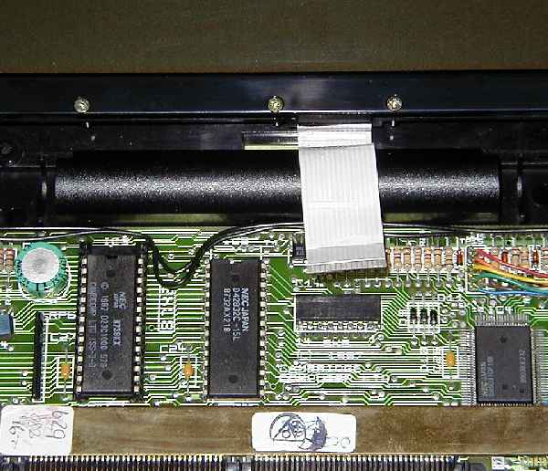
These are the only fixings, and purely friction holds the parts together. You should very carefully pull out the ribbon connector of the Epson display unit, from its black socket at the middle of the board, so it can be removed.
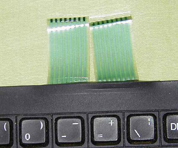
Now the keyboard must be removed and again care must be taken in gently pulling out it’s two ribbon connectors.
Ease the two battery springs from off their mounting, and slip the 9 pin D socket out of it’s recess, and then the main board should just pull over its mounting pillars and come out as a single unit. Handle it carefully, static isn’t a real problem with the whole unit, but you should avoid touching any of the exposed contacts, particularly for the expansion slots, as these can be easily oxidised by sweaty finger contact, and made less reliable.
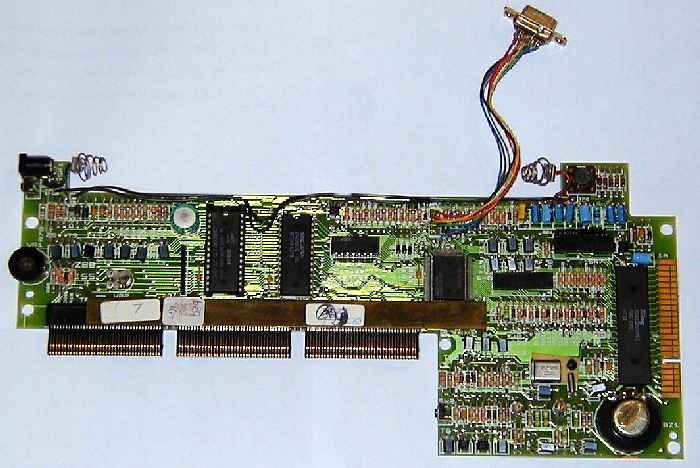
On my series 4 board, see below, the ROM (on the left ) is in the lower part of a 32 pin socket, whilst the 28 pin RAM chip is directly soldered in. The existing ROM is thus easily removed by being levered out of it’s socket with the aid of a small straight edge screw driver. If you look closely at the top of the RAM, you can just see in the photo, the white lines, of the top of a 32 pin chip outline, together with the four extra holes, currently filled with solder. The latter holes are fully connected, so the board was designed for a possible upgrade to the largest memory available at the time, which was 1Mb = 128K chip. Only 32K was installed, purely on cost grounds, the larger capacity chips could have almost doubled the cost of manufacture! However, it is for this reason that OZ version 3, the last in production machines, readily recognises 128K, but not 512K, for which you need a version 4 ROM, as well as modification of the main board.
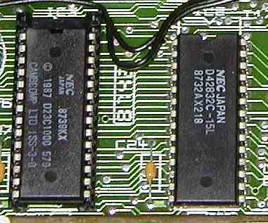
Now to the nitty gritty, that is desoldering the RAM chip. The easy route is, to snip off the pins of the chip, and then with a soldering iron, melt the solder, and pull out the remains of the pins with a pair of tweezers. The more difficult, is to attempt to desolder, using a solder pump. It is probably best to support the board vertically, then heat each pin , from the chip side, at it’s base. Wait until you see the solder melt on the base, then place the nozzle of your solder sucker / pump completely over the end of the pin and trigger it. With luck, all of the solder will be removed. At the same time remember to remove the solder from the 4 extra holes! Once all of the holes are clear, put in place the 32 pin, turned pin, low level DIL socket. You really do need the turned pin socket. The cheaper, compression fitting has a much higher profile, which with the chip fitted, will stop the keyboard sitting level. Before soldering it in, make sure that you have put it in the right way round. The indentation in the top bar of the socket should be lined up with a similar indent in the white silk screened chip outline. It doesn’t really matter, but we might as well get every thing in it’s correct position, you then don’t have to think too hard when putting in the new chip! Do use a soldering iron with a small sharp head, and make sure that you see the solder flow into the hole, as we don’t want any dry joints. Take care not to use too much solder, as we don’t want to create any short circuits with other pads / tracks.
As already mentioned I started out by merely replacing the RAM chip with a 1M static RAM. These come from RS in a plastic chip carrier. The pressure of the pins makes these bow outwards. Press this in to make the sides parallel, which will better align the pins with the socket. Then locate one side of the pins, in the correct orientation, into the socket. If you then push back against this side of the socket, you will be able to slip in the other side: once located, fully push the chip in. Note, that I have not bent out pin 30, as recommended in some accounts. This would be pin 28 of the original chip and hence the +5 volt supply. I noticed in the chip documentation, available as a previously mentioned PDF, that pin 30 of the Samsung RAM is in fact chip enable, CE, which is active high. The chip won’t work at all if there is not five volts on this pin. The only time that this line should go low is when the chip goes into suspend mode. I am looking into generating an appropriate signal for this, as the power consumption of the chip is minimal when in this mode, which should be when the computer is actually switched off.
Before any re-assembly, the case needs modification. The under side of the keyboard has a series of diagonal and box shaped ribs to stiffen it. These have already been removed during manufacture to allow for the extra height of the EPROM in it’s socket. We must make a similar modification, to take account of the RAM chip in it’s socket. For this I used a small pair of end cutter pliers. It was easy to snip through the quite soft plastic.
We are now in the position to re-assemble. I have not mentioned replacing the ROM, as I would like to see that it works, before screwing all back together again. An application of Occam’s razor, if it doesnt work, we have reduced the number of variables to one, by replacing just the RAM! We can reconnect everything, without screwing the case together. Take great care when refitting the tongues of the display and keyboard ribbons. They must not be cracked, and this is easy to do if you bend the ribbon through too sharp an angle, Some pressure is needed to refit, particularly the keyboard ribbons. Once all is reconnected, plug in the powersupply, batteries will not fit without complete assembly, and the screen should flash on, probably a blank, blue, shimmering display, which should clear once you have pushed the re-set button twice. If this is all you intend to do, re-assemble in the reverse order to disassembly on page two.
All images and text copyright Dr Colin F Parsons, May 2002